
Home>Create & Decorate>DIY & Crafts>How To Make Circuit Board
DIY & Crafts
How To Make Circuit Board
Published: June 4, 2024

Content Creator specializing in woodworking and interior transformations. Caegan's guides motivate readers to undertake their own projects, while his custom furniture adds a personal touch.
Learn how to make a circuit board with our step-by-step DIY guide. Explore fun and creative DIY & Crafts projects today!
(Many of the links in this article redirect to a specific reviewed product. Your purchase of these products through affiliate links helps to generate commission for Twigandthistle.com, at no extra cost. Learn more)
Introduction
So, you want to learn how to make a circuit board? Well, you've come to the right place! Making your own circuit board can be a rewarding and cost-effective way to bring your electronic projects to life. Whether you're a hobbyist or a professional, understanding the process of creating a circuit board from scratch can open up a world of possibilities for your DIY electronics projects. In this article, we'll take you through the step-by-step process of making a circuit board, from designing the layout to testing the final product. So, roll up your sleeves and get ready to dive into the exciting world of circuit board creation!
Understanding Circuit Boards
A circuit board, also known as a printed circuit board (PCB), is a crucial component in electronic devices. It serves as a platform for connecting and supporting electronic components to form a functional circuit. The board is typically made of a non-conductive material, such as fiberglass, with thin layers of copper foil laminated onto its surface. These copper layers are etched to create pathways for electrical currents to flow between components. The pathways, known as traces, are carefully designed to ensure proper connectivity and functionality of the circuit.
Circuit boards come in various types and sizes, ranging from simple single-layer boards to complex multi-layer boards. Single-layer boards have components and traces on only one side, while multi-layer boards have components and traces on both sides, connected through plated through-holes. The choice of board type depends on the complexity of the circuit and the space available within the device.
Understanding the basics of circuit boards is essential before diving into the process of making one. It's like laying the foundation for a building – a strong foundation ensures the stability and reliability of the structure. Similarly, a good understanding of circuit boards sets the stage for successful and functional electronic projects. Now that we have a grasp of what circuit boards are, let's move on to the next step – gathering the materials and tools needed for making a circuit board.
Materials and Tools Needed
When it comes to making your own circuit board, having the right materials and tools at your disposal is crucial. Here's a comprehensive list of what you'll need to get started:
Materials:
- Copper Clad Board: This serves as the base material for your circuit board, providing a conductive surface for creating the circuit traces.
- Etching Solution: A chemical solution, such as ferric chloride, used to remove excess copper from the board during the etching process.
- Acetone: Used for cleaning and degreasing the copper clad board before applying the circuit design.
- Permanent Marker or Toner Transfer Paper: For transferring the circuit design onto the board.
- Masking Tape: Helps in creating a protective barrier on the board during the etching process.
- Drill Bits: Essential for drilling holes to accommodate electronic components.
Tools:
- Computer and PCB Design Software: For creating and designing the circuit layout.
- Laser Printer: Used to print the circuit design onto the transfer paper.
- Iron: For transferring the circuit design from the paper to the copper clad board.
- Plastic or Glass Container: To hold the etching solution during the etching process.
- Safety Gear: Such as gloves and goggles, for protection during the etching process.
- Drill Press or Hand Drill: For drilling holes in the board as per the circuit design.
- Soldering Iron and Solder: For attaching electronic components to the board.
Having these materials and tools ready will set you up for a smooth and efficient circuit board creation process. Now that you have everything you need, it's time to move on to the exciting part – designing the circuit board!
Designing the Circuit Board
Designing the circuit board is a critical phase in the process of creating a functional and efficient electronic circuit. This phase involves translating the schematic diagram of the circuit into a physical layout that can be implemented on the board. Here's a step-by-step guide to designing the circuit board:
-
Schematic Diagram: Begin by creating a schematic diagram of the circuit using specialized software such as Eagle, KiCad, or Altium Designer. The schematic diagram represents the electrical connections between components and serves as the blueprint for the physical layout.
-
PCB Layout: Once the schematic is complete, use the same software to convert the schematic into a PCB layout. This involves placing the components on the board and routing the connections between them. Pay close attention to the placement of components to ensure efficient use of space and minimal signal interference.
-
Traces and Signal Integrity: When routing the connections, consider the signal integrity of the circuit. Ensure that high-speed signals have controlled impedance traces and that signal paths are kept as short as possible to minimize signal degradation.
-
Power and Ground Planes: Create dedicated power and ground planes on the board to provide stable voltage and minimize noise. This involves allocating specific areas of the board for power and ground connections, ensuring a robust and stable power distribution throughout the circuit.
-
Component Placement: Carefully place the components on the board, considering factors such as heat dissipation, accessibility for soldering, and overall circuit functionality. Group related components together to minimize trace length and optimize the layout.
-
Design Rule Check (DRC): Before finalizing the design, run a design rule check to ensure that the layout complies with manufacturing and assembly requirements. This step helps identify potential issues such as trace spacing violations, component clearance violations, and other design rule infractions.
-
Finalizing the Design: Once the layout is complete and passes the design rule check, review the design for any potential improvements or optimizations. Consider factors such as board size, component placement, and manufacturability before moving on to the next phase.
By following these steps, you can create a well-organized and optimized circuit board design that forms the foundation for a successful electronic project. With the design in place, the next step is to transfer the design onto the board and prepare it for the manufacturing process.
Transferring the Design to the Board
Transferring the circuit design from the computer onto the copper clad board is a crucial step in the circuit board creation process. This phase involves accurately replicating the circuit layout onto the board to prepare it for the subsequent etching and component placement. Here's a detailed guide on how to transfer the design to the board:
-
Print the Circuit Design: Begin by printing the finalized circuit board layout onto a special transfer paper using a laser printer. The design should be printed in a mirrored format to ensure that it transfers onto the copper clad board correctly.
-
Prepare the Copper Clad Board: Clean the copper clad board thoroughly using acetone to remove any dirt, grease, or oxidation. This step is essential to ensure proper adhesion of the transferred design onto the board.
-
Transfer Method 1: Toner Transfer Paper: If using toner transfer paper, place the printed design onto the copper clad board with the toner side in contact with the copper surface. Apply heat and pressure using a hot iron to transfer the toner from the paper onto the board. This process effectively transfers the circuit traces and component outlines onto the board.
-
Transfer Method 2: Permanent Marker: Alternatively, if using a permanent marker, carefully trace the circuit design onto the copper clad board, ensuring precision and accuracy in replicating the traces and component outlines. This method requires steady handwork and attention to detail.
-
Inspect the Transfer: Once the transfer process is complete, carefully inspect the transferred design to ensure that all traces and component outlines are accurately replicated on the board. Any missing or incomplete transfers should be addressed before proceeding to the next phase.
-
Protective Masking: After the design is transferred, use masking tape to create a protective barrier around the edges of the board. This helps prevent the etching solution from affecting areas outside the intended circuit layout during the etching process.
By following these steps, you can effectively transfer the meticulously designed circuit layout onto the copper clad board, setting the stage for the subsequent etching process. With the design successfully transferred, the next phase involves etching the board to remove excess copper and reveal the circuit traces.
Etching the Circuit Board
The process of etching the circuit board is a crucial step that involves removing excess copper from the board, leaving behind the desired circuit traces. This selective removal of copper is achieved through the use of an etching solution, typically ferric chloride. Here's a detailed guide on how to etch the circuit board effectively:
-
Prepare the Etching Solution: Begin by preparing the etching solution in a well-ventilated area. Ferric chloride is a commonly used etchant and is available in crystal or liquid form. Follow the manufacturer's instructions to prepare the solution, ensuring the correct concentration and temperature for optimal etching.
-
Etching Container: Pour the prepared etching solution into a plastic or glass container that is large enough to accommodate the circuit board. It is important to use a container made of a material that is resistant to the corrosive nature of the etchant.
-
Etching Process: Carefully place the transferred circuit board into the etching solution, ensuring that the copper side of the board is fully submerged. Agitate the container gently to facilitate the etching process, allowing the solution to dissolve the unwanted copper from the board.
-
Monitor the Etching: Periodically inspect the board to monitor the progress of the etching process. The solution will gradually eat away the exposed copper, leaving behind the circuit traces. The etching time can vary based on the concentration of the solution and the thickness of the copper layer.
-
Safety Precautions: It is essential to take safety precautions during the etching process. Wear protective gloves and goggles to prevent direct contact with the etchant, and work in a well-ventilated area to avoid inhaling fumes. Additionally, handle the etching solution with care to prevent spills and splashes.
-
Neutralizing the Solution: Once the etching is complete and the unwanted copper has been dissolved, carefully remove the board from the etching solution. Rinse the board thoroughly with water to stop the etching action and neutralize any remaining traces of the etchant.
-
Inspect the Etched Board: After neutralizing the board, inspect the etched circuit traces to ensure that they are well-defined and free from any residual copper. Any imperfections or incomplete etching should be addressed before proceeding to the next phase.
By following these steps, you can effectively etch the circuit board, revealing the meticulously designed circuit traces that form the foundation of the electronic circuit. With the board successfully etched, the next phase involves drilling holes and adding components to bring the circuit to life.
Drilling Holes and Adding Components
After successfully etching the circuit board, the next crucial step is to drill holes and add components to bring the circuit to life. This phase involves creating openings for electronic components and securely mounting them onto the board. Here's a detailed guide on how to drill holes and add components effectively:
-
Drilling Holes: Begin by identifying the locations where components will be mounted on the board. Use a drill press or a hand drill equipped with a small-diameter drill bit to carefully create holes at precise locations as per the circuit design. It's essential to use the correct drill bit size to accommodate the leads of the components without causing damage to the board.
-
Component Placement: Once the holes are drilled, proceed to place the electronic components onto the board. Ensure that the components are oriented correctly and aligned with their designated positions. Group related components together based on their functions to streamline the assembly process and minimize wiring complexity.
-
Soldering: With the components in place, use a soldering iron and solder to establish electrical connections between the component leads and the circuit traces. Apply a small amount of solder to each connection point, ensuring a secure and reliable bond between the components and the board. Exercise caution to prevent solder bridges or cold joints that can compromise the circuit's functionality.
-
Trimming Excess Leads: After soldering the components, trim any excess leads using wire cutters or flush-cutting pliers. This step helps maintain a neat and organized appearance of the circuit board while preventing potential short circuits caused by protruding leads.
-
Inspecting the Assembly: Once all components are soldered and excess leads are trimmed, carefully inspect the assembly to ensure that all connections are secure and free from soldering defects. Look for any potential solder bridges, cold joints, or misplaced components that may require rework.
By following these steps, you can effectively drill holes and add components to the circuit board, transforming it from a bare substrate into a functional electronic circuit. With the components securely mounted and interconnected, the next phase involves testing the circuit board to validate its functionality and performance.
Testing the Circuit Board
Testing the circuit board is a critical phase that ensures the functionality and performance of the newly assembled electronic circuit. This phase involves subjecting the circuit board to a series of tests to verify its electrical connectivity, signal integrity, and overall operational behavior. Here's a detailed guide on how to test the circuit board effectively:
-
Visual Inspection: Begin by conducting a visual inspection of the assembled circuit board. Look for any soldering defects, such as solder bridges, cold joints, or misplaced components. Ensure that all components are securely mounted and that there are no visible signs of damage or short circuits.
-
Continuity Testing: Use a multimeter set to the continuity test mode to check for electrical connectivity between various points on the circuit board. Verify that the traces, pads, and component leads are properly connected as per the circuit design. Any unexpected open or short circuits should be identified and addressed.
-
Power-Up Test: Power up the circuit board using a suitable power supply within the specified voltage and current ratings. Monitor the board for any signs of abnormal behavior, such as excessive heat, smoke, or unusual odors. Verify that the power distribution is stable and that the components are receiving the expected supply voltages.
-
Functional Testing: If the circuit board is part of a larger system, perform functional testing to validate its intended operation. This may involve inputting signals, data, or control commands to assess the board's response and output behavior. Verify that the circuit functions as expected and performs its designated tasks accurately.
-
Signal Integrity Testing: For circuits involving high-speed signals or sensitive analog components, conduct signal integrity testing to ensure that the signals propagate without distortion or degradation. Use oscilloscopes, signal generators, or spectrum analyzers to analyze the quality of the signals at various points on the board.
-
Load Testing: If the circuit board interfaces with external devices or loads, perform load testing to assess its ability to drive the connected loads. Verify that the board can deliver the required currents and voltages without experiencing voltage drops, excessive heating, or instability.
-
Environmental Testing: Depending on the application, consider subjecting the circuit board to environmental testing, such as temperature cycling, humidity testing, or vibration testing. This helps assess the board's reliability and performance under varying environmental conditions.
By following these testing procedures, you can effectively validate the functionality, performance, and reliability of the circuit board. Any identified issues or anomalies should be addressed through troubleshooting and corrective measures to ensure that the board meets the desired specifications and standards. With the successful completion of the testing phase, the circuit board is ready for integration into the intended electronic system or device.
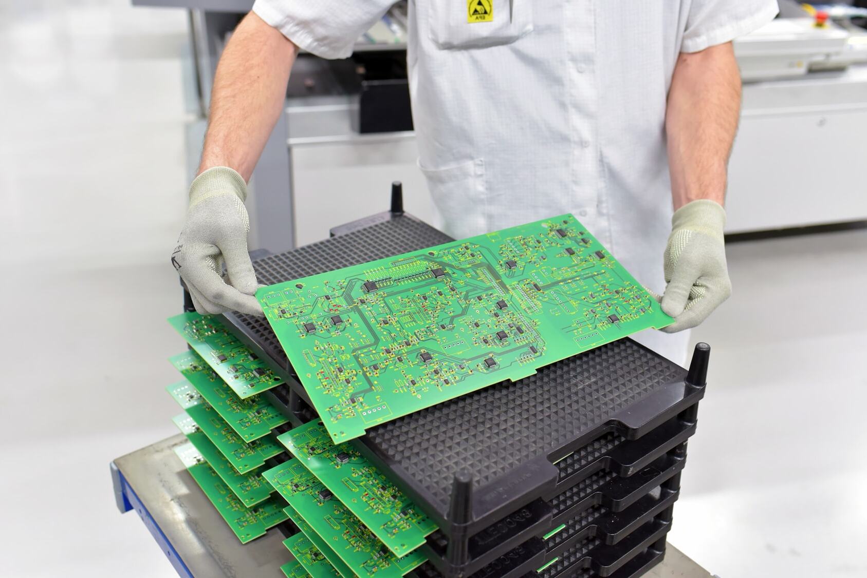
Finalizing the Circuit Board
After successfully testing the circuit board and addressing any identified issues, the finalization phase focuses on preparing the board for integration into the intended electronic system or device. This involves a series of steps to ensure that the board is ready for deployment and meets the necessary criteria for functionality and reliability.
-
Cleaning and Inspection: Begin by thoroughly cleaning the circuit board to remove any residues, flux, or contaminants that may have accumulated during the assembly and testing processes. Use a gentle cleaning solution and a soft brush to ensure that the board's surface is free from any foreign particles. Once cleaned, conduct a final visual inspection to verify that the board is in pristine condition and ready for integration.
-
Protective Coating: Consider applying a protective coating to the circuit board to safeguard it against environmental factors, moisture, and mechanical stress. Options for protective coatings include conformal coatings, acrylic resins, or silicone-based coatings. The chosen coating should provide insulation, corrosion resistance, and protection against dust and debris, enhancing the board's longevity and reliability.
-
Labeling and Documentation: It is essential to label the circuit board with pertinent information such as part numbers, revision codes, and functional descriptions. Additionally, prepare comprehensive documentation that includes the board's specifications, assembly instructions, and testing procedures. Clear and detailed labeling and documentation facilitate future maintenance, troubleshooting, and replacement of the board if necessary.
-
Packaging and Storage: Once the circuit board is finalized, carefully package it in suitable antistatic packaging to prevent electrostatic discharge (ESD) damage. Store the board in a controlled environment with stable temperature and humidity conditions to maintain its integrity. Proper packaging and storage help preserve the board's functionality and prevent degradation over time.
-
Integration and Deployment: Finally, integrate the finalized circuit board into the target electronic system or device, following the specified installation procedures. Ensure that the board is securely mounted and connected as per the system requirements. Conduct a final verification to confirm that the board operates seamlessly within the larger electronic system, meeting the intended functionality and performance criteria.
By completing these finalization steps, the circuit board is fully prepared for deployment and integration into the intended electronic application. The meticulous attention to detail in finalizing the board ensures its reliability, longevity, and seamless operation within the broader electronic system.